Wrapping up the Alarm Clock Project

It has been a long while since the last post. Amongst other things, the clock has been a work-in-progress. Each time I made some progress, I found some new reason to create a revision. The initial revisions where based on issues and oversights. I am finding that as the project matures, the nature of the revisions are changing. Earlier on I was focused on just seeing things working i.e. how to program the micro with the ISP, how to get the modules to communicate. The earlier boards were either bound to the original dev-board, bread board or both. Now, I have the display module and the main-board untethered from the bread board and they are happily working with each other. Each step of the way I learn something new and those earlier issues are no longer the obstacles that they were. So much so that the problems and challenges I face now are more functional and mechanical.

I now have a basic board layout for the controller and the display that I am happy to progress with. These are certainly not the cheapest options, but as I may have mentioned before, they offer a way for me to learn about and demonstrate inter processor communication as well as dealing with multiple voltages in the one application. My focus now was to get the job finished. I see two basic challenges. 1. Getting everything into the case and 2. Getting the alarm working!

Low Profile 7-Segment Display

img_0268e

The seven segment displays I had been using would not allow me to mount the display in the case. It was time to search for a better solution. I discovered some thin profile seven segment displays. They are perfect for the job, though they are a bit tricky to solder since they do not have any leads. I worked around that with a piece of lead wire inserted in two of the holes in my board. This enabled my to apply light pressure on the display in the direction of the leads to hold them firm in position for soldering. Then allowed all the displays to be identical.

Alarm

The alarm buzzer then became my biggest challenge and something new to learn about.The clock originally had a Piezo buzzer. Since the goal is to restore the clock, I was hoping to use a Piezo again. However the results from testing were not what I had expected. It was really difficult to get any sort of appreciable sound. Admittedly, the simple Piezo need to be properly mounted in order to resonate correctly. This I could not really achieve with my test set-up.

Testing the Piezo and looking generally at buzzers was opening up a new avenue of concepts to learn. I found the theory simple enough and meant I still had some design decisions to make. The first thing was to understand what direction to take. Since this was new territory, I saw no other avenue but to order some different types and just try them out. The basic criteria I set was capable of handling at least 5V and in around the 90dB range. I have to admit, I had no idea what 90dB was going to give me.

Description Manufacturer Part Number Digi-Key part Number
Zero-Peak Signal Buzzer Single Tone 2.67kHz Magnetic 0~5V 88dB @ 3V, 10cm TDK Corporation CSQG703BP 445-4832-1-ND
Zero-Peak Signal Buzzer Single Tone 2kHz Magnetic 2~4V 85dB @ 3V, 5cm CUI Inc. SDR08540M3-01 102-1286-ND
Zero-Peak Signal Buzzer Single Tone 2.4kHz Magnetic 3~8V 87dB @ 5V, 10cm CUI Inc. CT-1205-SMT-TR 102-1199-1-ND

In choosing, I had the choice to use a device that need no external driver or to drive the buzzer myself. I opted for the second to also learn how to integrate the PWM feature of the micro into the solution. In testing the buzzers, I could mount the CSQG703BP directly on my bread board. For the other two I created a (rough) test harness and used a Gabotronics Xminilab as my signal source – I don’t possess a bench signal generator yet.

img_0270e

The CSQG703BP tested OK but the tone was quite weak. I could not get a tone out of the SDR08540M3-01 at all but that could be related to the set-up I had. Although the  CT-1205-SMT-TR was quite bulky in comparison to the others, it delivered the best results.

I made the final revision to the board to take the CT-1205-SMT-TR on the underside over the place where the Piezo was originally. The case had a moulding that gave more than enough space for this part, so I was lucky there.

In “bringing up” the buzzer, I had to learn about PWM control and what that meant. I created a test program to only operate the buzzer and not worry about the whole clock functionality yet. In the end I thought it would be cute if the alarm would not simply make the traditional chirps but send  the message “WAKE UP” in Morse code.wakeup

Buzzer Alias Portb.1
Config Buzzer = Output
' CTC-Mode for ~ 2.5kHz
Config Timer1 = Timer , Compare A = Toggle , Prescale = 1 , Clear Timer = 1

Const Timer0_startvalue = 100                               ' 0.001 seconds
Config Timer0 = Timer , Prescale = 64
Timer0 = Timer0_startvalue
On Timer0 Timer0_isr
Enable Timer0
Start Timer0
Enable Interrupts

Heartbeat Alias Portc.3 ' LED indicator
Config Heartbeat = Output : Heartbeat = 0
Const Tone_pitch = 200

Dim Tone As Byte
Dim Tone_length As Integer
Dim Tone_idx As Byte
Dim Song(40) As Byte
Dim Songlen As Byte
Dim Song_finished As Bit

Const Base_length = 7

' Load the song - Songlen should be used to know the length afterwards.
Wait 5
Songlen = 0
Restore Melody
Do
   Read Tone
   If Tone <> &HFF Then
      Incr Songlen
      Song(songlen) = Tone
   End If
Loop Until Tone = &HFF
Tone_length = 1

' A wake up signal. Illuminate the LED for one second.
Set Heartbeat
Wait 1
Reset Heartbeat

' Play the "song" every 10 seconds
Do
   If Song_finished = 1 Then
      Wait 10
      Tone_idx = 0
      Reset Song_finished
   End If
Loop
End

Buzzer_on:
   Compare1a = Tone_pitch
   Tccr1a.6 = 1
Return

Buzzer_off:
   Tccr1a.6 = 0
Return

' ISR for timer 0. This will traverse the "melody" playing each tone, and pause
' in turn until the end of the song.
' The Melody is a series of data values. Since there is only one tone from the 
' buzzer, only the length is given. There is a base length and the tone length is
' a multiple of that. Basically this comes from Morse code that the dots are three
' units long and the dashes are seven. Anything greater than &H80 is considered 
' a pause.
Timer0_isr:
   Timer0 = Timer0_startvalue
   If Tone_length > 0 Then
      Decr Tone_length
      If Tone_length <= Base_length Then
         Gosub Buzzer_off
      End If
   Else
      Toggle Heartbeat
      If Tone_idx < Songlen Then          Incr Tone_idx                            ' Get the next tone          Tone = Song(tone_idx)          Tone_length = Tone And &H0F              ' Get the tone length          Tone_length = Base_length * Tone_length  ' Factor the tone buy the base length          Tone_length = Tone_length + Base_length  ' Build in a unit gap at the end          If Tone > &H80 Then
            Gosub Buzzer_off
         Else
            Gosub Buzzer_on
         End If
      Else
         Set Song_finished
      End If
   End If
Return

Melody:                                             ' Wake up - Morse code
Data &H01 , &H03 , &H03 , &H83 , &H01 , &H03 , &H83 , &H03 , &H01 , 
     &H03 , &H83 , &H01 , &H87 , &H01 , &H01 , &H03 , &H83 , &H01 , 
     &H03 , &H03 , &H01 , &HFF

Alarm Integration

It was easy enough to integrate the alarm-tone code into the main-board code since since the 16-bit Timer0 was not in use. I could configure the Timer0 for CTC-Mode (Clear Timer on Compare) to deliver the 2.5kHz which produced the best results. I did attempt other PWM configurations but the results were not what I was expecting or wanted.

Config Timer1 = Timer , Compare A = Toggle , Prescale = 1 , Clear Timer = 1
Const Tone_pitch = 200

In my original design, I had anticipated to utilise the alarm interrupt (address $E) that the RTC-DFC supports – or is meant to support. I actually found that this does not work. When the alarm is programmed, it can be seen to be fired since the indicator LED on the module will illuminate. However, the Alarm Interrupt line is not brought low and therefore not detected in my code. I have two modules to try this out on and neither would pull the interrupt line low – even after upgrading to the latest firmware.

After chatting with my tutor, Chris Gammell from Contextual Electronics, I came to realise the workaround. In addition to the Interrupt line, it is possible to detect the alarm in the interrupt status register. This works. So I modified the code not to rely on the interrupt line but to, instead, query the Interrupt Status Register and invoke the alarm if the alarm bit is set.

Read_dfc_interrupt_flag:
   Reset Dfc_ss
   Mosi(1) = &HCE
   Spiout Mosi(1) , 1
   Spiin Mosi(1) , 1
   Set Dfc_ss
   Interrupt_register = Mosi(1)

   If Alarm_disabled = 0 Then
      Temp = Interrupt_register And &B00000100
      If Temp = &B00000100 Then
         Set Alarm_fired
      End If
   End If
Return

Wrapping up

I was keen to get this project into a finished state. The enabling of the alarm was one of the last stages. All was needed then was to clean up the code a bit and implement an “alarm cancel”. There is a push-button on one of the front feet so that the alarm can be cancelled by tapping the top of the clock.

img_0274eSo here it is, the renovated clock. I utilised the BOM feature of KiCad to perform a cost analysis of the two modules. The Clock module comes to a BOM cost of 41.46€ (including the RTC-DFC from ELV) and the display module comes to a BOM cost of 35.14€. I have already mentioned that this implementation is a bit over the top in terms of components etc. but it is more about the learning exercise rather than making a cost effective clock and display module.

Just to recap on what I have learned in this exercise:

  • Circuit design
  • PCB layout
  • PCB Manufacturing
  • Assembly
    • Improved through-hole soldering
    • SMD
  • Programming through an ISP (to a development board and my own board)
  • Inter module programming using I²C and SPI
  • Trouble shooting using a logic analyser and oscilloscope

img_0275e

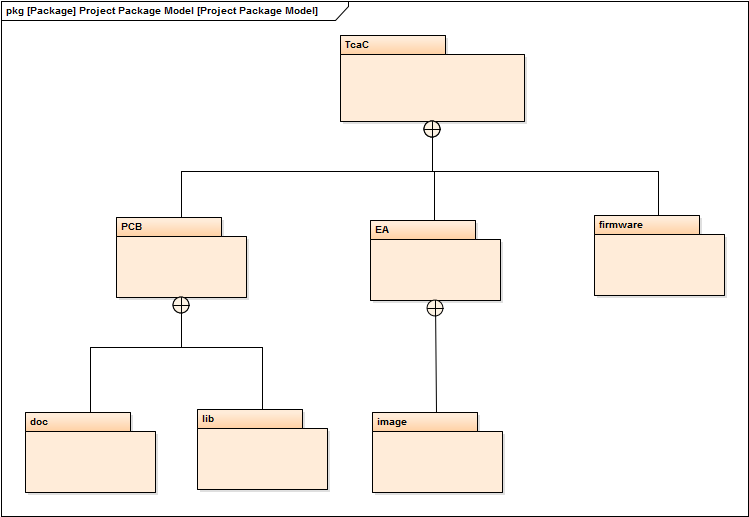
When I set out on this project, I anticipated to learn a bit about UML – SysML in particular. I did start out that way but with everything else I had to learn on the way, it sort of went by the way. However the block diagrams that I created ended up being an valuable reference of what I had intended the pin allocations to be. That is something will try to utilise more for the next project.

Addendum

Now that the clock has been running a week or so, I was thinking about how it is able to pick up the time signal better in some places than others. I was made think about this further when the ELV Journal showcased an external antenna for the RTC-DCF. I realised that all this time, I have been treating the DFC-RTF as a black box an literally taking it for granted. That approach certainly helped to get the job done. It was time to take a closer look. The RTC-DFC is a module in two parts. A DCF77 receiver module and a micro based RTC. It turns out that I really had a bit of luck with the positioning of the antenna on the main board. In certain locations the clock can (eventually) receive a signal, in others not at all. Looking at the data signal from the DCF77, I could clearly see the one second pulses when the antenna was about 5cm from the board. Bring the antenna closer and the signal is disrupted as the images below show.

It was not a light decision to take to add the external antenna to the clock as I had to make a slight modification to the case for the antenna cable. The performance of the clock as improved immensely. It now sits, as a trophy, on my Lab windowsill.

Further testing the μController Display Module

In the last post, I was able to get the μController version of the display module working with a basic test routine that proved that 1. the controller could be programmed and 2. the display was being driven correctly. The next stage is to flesh this out to replicate the MAX2771 API. The purpose here is not to simply create a duplicate of the MAX2771 which does a great job on its own. This approach means that I can re-use the code I created for the MAX2771 display module project. The additional goal of this small project was to gain experience in creating a SPI slave! Interfacing with the MAX2771 was simple since that is already a SPI slave unit. All I needed was to just create the master.

Connecting things together

I still have things set up from the previous tests so it was just a matter of connecting things back up again. Though this time I had two units to program instead of just one. I still have the main controller board for the clock to complete so I used the myAVR Dev board as a provisional main controller. Luckly, the myAVR dev board comes with its own programmer. I had to program this via the myAVR ProgTool since the BASCOM-AVR IDE was in use with programming the display module via the AVRISP mkII. It sounds more awkward than what it turned out to be. The part that was awkward was that the AVRISP mkII had trouble programming the display module while the SPI connection was still made to the myAVR dev board (my provisional mainboard). I had to disconnect the /SS, MOSI and CLK from the display module before being able to program. This would be a point of research to work out what is involved to be able to program the display module while still connected!

μControlled Display Driver Integration Test

Once the infrastructure of programmers and connections was sorted, it was just then a matter of piecing together the code to enable the slave unit to start servicing the requests of the master i.e to start displaying the time. With the Real Time Clock still connected (via an I2C bus) I had a neat source of test data.

Getting thing up and running was rewarded with a red blinking LED on the dev board. This was my signal that the communication with the Real Time Clock was functioning. The next was the display module itself.To keep things simple,  I am opting to use the basic BASCOM constructs for SPI. The logic analyzer was useful for seeing that the SPI messages were being sent. Though my particular logic analyzer only shows that there was activity. It lacks the sophistication of being able to see exactly what was being sent. Thankfully, I have been able to get things working without that level of sophistication.

LA6_Image_0020

Creating the Slave

Dim Rbit As Bit
Config Pinb.4 = Output                    ' MISO
Config Spi = Hard , Interrupt = On , Data Order = Msb , 
       Master = No , Polarity = Low , Phase = 0 , Clockrate = 128
Spiinit

On Spi Spi_isr Nosave

Enable Timer0
Enable Timer1
Enable Interrupts

The snippet above shows how the slave was defined. Basically I used the same construct in the master. The “Master = yes” property is the only difference. Once data is available for the slave to read, the spi_isr interrupt routine is executed. Here I just grab the data into a Regisiter array. The API I was wanting to implement was to read a two byte command i.e. a register address and then a value. I was not sure on how this is to be done since BASCOM-AVR documentation only really talks about receiving one byte at a time for slave. In comparison, sending multiple bytes from the master is not difficult at all.

Spi_isr:
   PUSH r24    ; save used register
   IN r24, SREG; save SREG
   PUSH r24
   Set Rbit                         ' we received something
      If Spi_idx = 0 Then
         Idx = SPDR
         Set Spi_idx
      Else
         Register(idx) = SPDR
         Reset Spi_idx
      End If
   POP r24
   !OUT SREG, r24 ; restore sreg
   POP r24       ; and the used register
Return

Here I had a variable to track which element of the command was being received spi_idx. When reset, then the first value from the master is expected and therefore that value is recorded as an index value i.e the register address. When spi_idx is set, then it is expected that the value from the master is the register value and that is then directly recorded in the Register array.

With the register address and value for the register obtained from the master, then it was a matter of interpreting the newly arrived information. I implemented this using a case construct.

   If Spi_idx = 0 Then
      Select Case Idx
         Case Hours_10:
            Digits(1) = Register(idx)
         Case Hours_unit:
             Digits(2) = Register(idx)
         Case Minutes_10:
            Digits(3) = Register(idx)
         Case Minutes_unit:
            Digits(4) = Register(idx)
         Case Colon:
            Digits(5) = Register(idx)
         Case Indicators:
            Digits(6) = Register(idx)
         ' Case Intensity:
         ' Case Power_mode:
         Case Digit_blink:
             Blink_mask = Register(idx)
         ' Case Blink_rate:
         Case Test_mode:
            If Register(idx) = Enabled Then
               Digits(1) = 8
               Digits(2) = 8
               Digits(3) = 8
               Digits(4) = 8
               Digits(5) = 8
               Digits(6) = 8
            Else
               Digits(1) = 0
               Digits(2) = 0
               Digits(3) = 0
               Digits(4) = 0
               Digits(5) = 0
               Digits(6) = 0
            End If
         Case Else
      End Select
      End If
   End If

The idea here is to simply  react if there is a new value arrived. Based on the value of idx (the register address) to then assign the value from the register to a variable that will result in the desired behaviour. i.e. setting a digit value etc.

One feature I have implemented that is not part of the MAX2771 API is a Blink feature. i.e. to enable a digit or colon to blink. I managed this with a mask with one bit for each element of the display. This seems to work quite well.

Renderdisplay_isr: 
   Timer0 = Timer0_count
   Incr Position
   If Position > 5 Then
      Position = 0
   End If

   Digit = Position + 1
   PORTD = &H0A          ' Set all segments off
   PORTC = Makebcd(position)

   Blink_test = &B00000001
   Shift Blink_test , Left , Position
   Blink_test = Blink_test And Blink_mask
   If blink_flag = 1 and blink_test > 0 Then
      Value = Digit_off
   Else
      Value = Digits(digit)
   End If
   PORTD = Value
Return

Next Steps

The μController version of the display module is working, I have to admit, in principle. There is still a bit more work to do to clean up its behaviour and possibly implement more tests and features i.e. the indicators on the top and bottom left of the display.

The actual main board still needs to be done. This will be presented in future posts. There are some considerations to be done with that in terms of its physical size for the existing casing. Another task that is outstanding is the interfacing of the Real Time Clock with SPI rather than I2C. I have been using I2C since that is what I used on the very first trial. My goal is to have a multiple slave SPI implementation. This too can be prototyped with my current set up before finalising on the actual main controller board.

The advantage I have with the current approach is that the firmware for the main board is progressively being done with the testing of the modules. It is just missing the implementation of the various push buttons. Even this can be implemented in the myAVR Development board.

Wired for Action – almost

In the last post, I presented the initial ideas for powering the project. Now it is time to move on and start looking into the individual modules. I was impressed as to how quickly this part progressed since I had done the up-front thinking of the pin and port allocation. So much so, that before I knew it I had most of the schematic done making it unnecessary to span the development over several blog posts.

sch-top-02The high level diagram is now looking more complete with the use of hierarchical sheet pins to connect the respective module. This clearly demonstrates the communication between the modules and again, looks very similar to the initial block diagram. It should be iterated that the up-front work of the block diagram contributed significantly to the creation of this section of the schematic. Since I had previously thought out the pin and port allocation, it was a simple matter of aligning the labels on the sheets so that it is concise and descriptive.

Controller

The controller chosen for this project is the ATMega88p. I have to admit for no good reason other than I have a development board for this processor and have used the ATMega8 before. Unless there is a significant reason to re-think this decision, I will be staying with the ATMega.

sch-controller-01

The controller diagram, at this stage, describes the connection of the Serial Peripheral Interface (SPI) bus and interrupts using hierarchical labels. I have also added a pin header for on-board programming. I do need to clarify this further to be sure that this is the correct connection/mechanism for programming the chip on-board.

RTC Module

It has been mentioned often enough that a pre-fabricated module will be used for the Real-Time-Clock (RTC). This is the RTC-DCF from ELV. This module implements a RTC with built in calendar and has also a module to receive the DCF77 signal. When all things are working, then there is no need to set the time on the final clock appliance. It is envisaged that there will be a manual mode for the clock in cases where the signal is not received.

IMG_1054The symbol for the RTC in KiCad is a custom symbol for this module. Though the original kit is mounted in an Arduino shield type form factor, the module itself can be punched out and either soldered onto the application board or, as I envisage, connect it to the application board via a set of 2×6 pole pin headers.

sch-display-01

This schematic implements the level shifter mechanism to shift the +5V signal from the controller to a 3V3 signal that the RTC requires. The RTC supports a couple of different mechanisms for communication. In this case, I am opting for SPI. The usage of the signal lines look to double up. This is only because when one communication mechanism is chosen (programmed via a DIP switch on the module) the other lines are used to support the extra interrupt features of the module. For the implementation and features I require, not all connections are necessary. The Tx line, for instance will not be required in this case.

Thinking back on the SysML block diagram, the level-shifter was not clearly visible on the block diagram. It was certainly defined in the model and was specified as the type of port on the 3V3 SPI bus. What is also not clear not the SysML model is that the SPI 3V3 bus requires both Vbb and Vcc to operate since it has to convert the signal between the two.

What’s next

I am quite satisfied with the schematic so far. More needs to be done on the controller. The interface buttons and switches need to be added. Also some thought needs to go into the housing since four buttons and a switch are already available. What I am proposing requires some additional buttons for the extra features. I am sure my refurbishment of this appliance can include some modifications. At this stage, I don’t see it a major problem to add these at the back of the housing.

The next significant module is the display module. I have some initial thoughts on this but will save that for a future post.

Modelling First

I have mentioned about the re-working of an old alarm clock. In this post, I will be kicking the project off and introducing my efforts to model the requirements and project organisation in SysML. I will be using Systems Architect from Sparx Systems.

Project Organisation

The project organisation shows the directory structure of the project in the form of a package diagram. The project is organised into three areas. One for the Enterprise Architect repository, on for the PCB or KiCad files and a third area to contain the firmware source code. This project is also available from the GitHub repository.

The project structure for all development files.

Requirements

In order to organise and document the features and functions for the project, a list of definitive requirements are first modelled. They enable the features and functions to be created and considered in the context of these requirements to ensure that the final device will contain all the correct features and that they will function in an expected way. In reality, this diagram is not enough. Each of the requirement boxes contain further detail about their meaning. The basic requirements are clear, even trivial. The clock should have a Time Feature and an Alarm Feature. Under the Time Feature, the user should be able to set the time when not in auto-time mode. The user should also have a simple way to set summer/winter time when in manual-mode.

Under the Alarm Feature, the user should be able to set the alarm time, enable and disable the alarm and operate a sleep function when the alarm is sounded.

Hierarchical model of the requirements

Block Diagram

The main block diagram contains the overview of the interconnecting modules of the whole clock system. It shows the power system that should deliver at least two levels – Vdd and Vb. These represent the +5V and 3.3V respectively to source the controller and the Real Time Clock module (RTF-DCF77). The RTF-DCF77 is a real time clock module that also incorporates capability to receive the DCF77 signal that is transmitted in Germany. This module has the capability of communicating with UART, I2C and SPI. The block diagram shows that communication will be established through a SPI bus. Three additional interrupts will be also implemented. The periodic interrupt (one second intervals), the DCF77 receipt interrupt and the alarm interrupt.

The micro controller (ATMega88) will have inputs from the device casing for the control buttons – implemented through InputPort D. The SPI bus will be implemented via the pins on the ATMega88 set side for this purpose i.e. Port B. An additional port will be used as the chip select 2 (/SS2) for the display module. Port C will be used to receive the interrupts from the RTF-DCF77 module.

Alarm Clock System

The SysML ports modelled as the SPI on the micro controller, the RTC-DCF77 and display modules are each of two types. A 5V version and a 3.3V version. The nested ports on the RTC-DCF77 are to also implement a level shifter to convert the 5V down to 3.3V. It is difficult to encapsulate this information without cluttering the diagram. What also seems a little unclear is the use of ST5 and ST6 nomenclature. These are the pin header labels on the actual physical module. Further information that would also be useful is the actual pin number on the pin header. I also figure that detail can wait for the schematic in KiCad.

System Interaction

Before I close this blog, I need to resist the urge to jump right into KiCad (and start doing some real work), to at least present a model regarding the internal interaction of the device. I believe this where the most time can be lost in SysML. The examples presented in the reference books are usually well contrived. Trying to fit the concepts into a simple case proves to be challenging. The idea is to model some behaviour behind the system block, parts and even use cases. The diagram presented below is a full state machine diagram for the alarm clock. This model was actually made some time ago and to save time, this time around, decided to import it into the new model since it is still a very close fit. There are some things missing like the interaction of the real time clock and enabling and disabling the alarm. I will add these in due time.

Alarm clock full state diagram

Under Systems Architect, this model can be simulated and you are able to see the execution through the various states when the various triggers are applied. This is another reason why a lot of time can be lost in this stage – you forget that the purpose is to model the behaviour and time is spent just getting the simulation working – but its fun. Since I already had this working model, I decided to import it and save that time.

The basic operation is to display the time. This will either be standard time or summer time. The rest of the model shows the interaction when various events are triggered, such as the time set button pressed and released.

Wrap-up

The SysUML model for the Alarm Clock project is by no means complete. Though I think I have provided enough at this stage for a project of this magnitude. The other models and definitions can and probably will be added as I move on with other aspects of the project. I am keen to get into the real hardware side and start to get things happening. In reflection I have to admit some things have come out in the exercise of modelling this in SysUML that I am grateful for.

  • I have a clear list of modules with clear requirements to develop and integrate into the final solution
    • Power system to deliver +5V and 3.3V
    • Display module
      • with indicators for auto-time and alarm enabled.
      • SPI capable
    • Real time clock. This is a given since I will be using the RTC-DCF77.
  • A clear allocation of the ports and interrupts of the micro controller before I start connecting and coding. This means I can start exploring the firmware already.

The state machine certainly needs some more re-work but this is enough for the first-cut.

Next Steps

The next steps will actually be to start working with KiCad. I don’t believe that a project of this size needs to be documented to death when the direction and requirements are known. As I said, I may well go back and correct and add some more diagrams where things are unclear and need further thinking/clarification. Research is also required for the display module. I do not have anything off-the-shelf for this so may have to consider to develop my own.